- Wed Jul 07, 2010 10:58 am
#104761
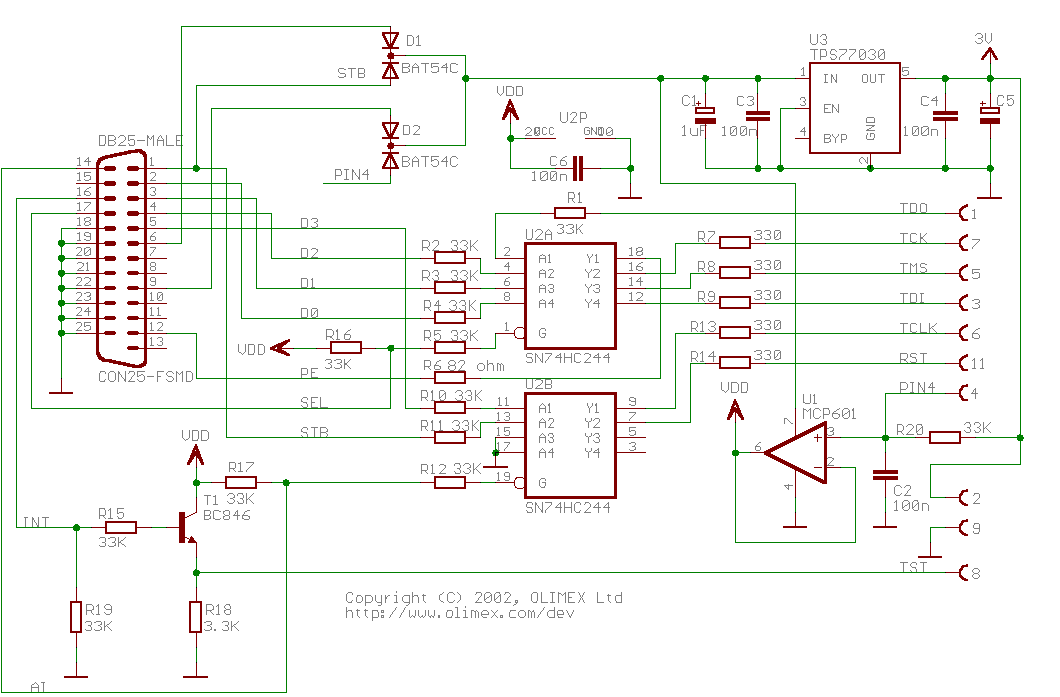
Hi, i'm trying to build the msp430-JTAG programmer with this schematic http://www.olimex.com/dev/images/msp430-jtag-d-sch.gif
Can somebody tell me what is the d1 adn d2 the pin 4 where does it go rom d2 and the pins form u2d where there are connected? because in the schematic is superimposed.
THanks!
Can somebody tell me what is the d1 adn d2 the pin 4 where does it go rom d2 and the pins form u2d where there are connected? because in the schematic is superimposed.
THanks!

