SparkFun Forums 

Where electronics enthusiasts find answers.

General project discussion / help
Did you make a robotic coffee pot which implements HTCPCP and decafs unauthorized users? Show it off here!
By dhoelzer
#166725
Hiya!

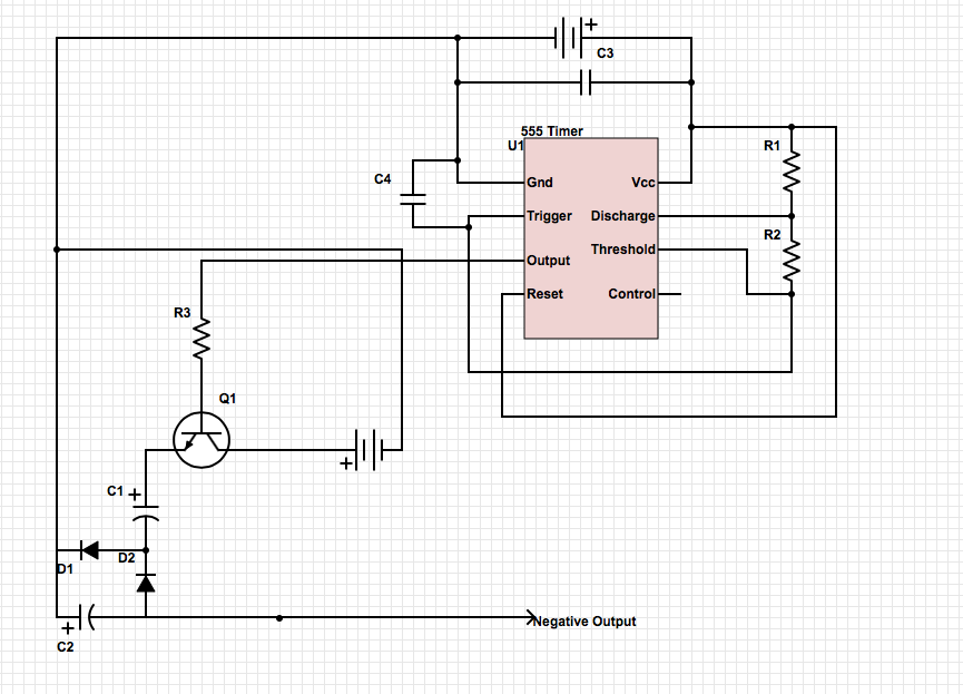
This is likely an extremely basic question for you folks. I have what I think is a simple voltage inverter that is intended to invert a 15 volt input via an NPN transistor being driven by a 555 timer with a couple of diodes and capacitors that I can then feed into a 7912 for a regulated -12 voltage. What I'm doing this for is to create a replacement +5/+12/-12 internal power supply for a vintage Apple Iic.

I've built the circuit and it sorta works, but my 555 is sizzling hot, so I think I've missed something. If you wouldn't mind having a look, I have an image of the circuit here:

Image

I'd appreciate any feedback. Sorry for the odd electrolytic cap widget; the tool didn't have a normal one in demo mode. :)
By Mee_n_Mac
#166737
Your image (schematic) didn't get stored or ??? Try again.

I'm surprised it's the 555 that's hot. :think:
By Programability
#166739
Off the top of my head the only two things I can think of is you 555 pin3 is shorting out but unlikely, the other is that you are powering it 15v, i know the datasheet says 15 or 18v but I've never been able to drive a 555 above 9v without complications.

If it is because you are running it at 15v but the supply is working then just get a little heatsink for the 555 or run it at a lower voltage and maybe add a transistor to do the switching from sub 12v to >12v.
By dhoelzer
#166740
Ah! I think I found the issue...

I had not put a resistor between the output of the 555 and the base on the transistor. Adding a transistor sorted it right out (heat issue).

I have a different issue now... While the charge pump is running, it settles in at -4.96 volts... I'm guessing that this is because I'm driving the transistor with the 5 volt output from the 555.. My intention, though, was to use that square wave to allow for -14 volts or so from the +15 volt input at the collector on the transistor.

Would I need to push the output from the 555 through a voltage doubler to increase the flow through the transistor and drive the negative voltage higher?

Thanks! Trying to add the schematic picture again:

Image
Programability wrote:Off the top of my head the only two things I can think of is you 555 pin3 is shorting out but unlikely, the other is that you are powering it 15v, i know the datasheet says 15 or 18v but I've never been able to drive a 555 above 9v without complications.

If it is because you are running it at 15v but the supply is working then just get a little heatsink for the 555 or run it at a lower voltage and maybe add a transistor to do the switching from sub 12v to >12v.
By Mee_n_Mac
#166743
I think there's at least 1 mistake in your schematic. Look at my red overlay below. C4, as drawn, is shorted out. Also are you missing a connection ? Lastly shouldn't CV be terminated w/a cap (0.01uF) to ground ?
inverter.png
You do not have the required permissions to view the files attached to this post.
By dhoelzer
#166744
Mee_n_Mac wrote:I think there's at least 1 mistake in your schematic. Look at my red overlay below. C4, as drawn, is shorted out. Also are you missing a connection ? Lastly shouldn't CV be terminated w/a cap (0.01uF) to ground ?
inverter.png
Hmmm... There is something wonky in that diagram. I'm looking at the circuit on a breadboard and it's definitely not shorted out. I'll have to redo the schematic and repost it.

Checking the data sheet I realized that I could power the 555 with upwards of 15 volts, so I am now powering it off of the 12 volt regulated supply that I also have available, but the voltage output is still hovering at about -6 volts. Interestingly, as soon as I power off the circuit, the negative voltage "rises" to about -9 volts and then decays to zero very, very slowly.

This type of charge pump circuit is very unfamiliar ground for me. I'm usually dealing exclusively with digital logic levels and supplying adequate levels to components, not working on designing a simple power supply. What is it, exactly, that regulates the maximum inverted voltage? Clearly, it's not the supplied voltage (meaning that I likely wasted time adding the NPN transistor to switch in a supply that wouldn't be limited by the maximum amperage available through the 555). Is it the pulse width frequency on the square wave?

Thanks!
By UhClem
#166745
There are a number of problems with the circuit as shown:

1) No current limit resistor on base of Q1.
2) Insufficient drive voltage on Q1. (emitter limited to less than 5V)
3) Will not work.

When Q1 is on you charge C3 but when Q1 turns off, that charge has nowhere to go. Normally you would use a push-pull driver so that you connect that node to ground when Q1 is off.

The topology of your switched capacitor circuit is also suspect. I am pretty sure it will never work.

What you want is:

Drive a capacitor (C1) with the output of the 555. The other lead of the capacitor is connected to two diodes: one diode with its cathode grounded (D1) and the other (D2) with its anode connected to the output capacitor. (C2, other lead to ground)

When the input is high, C1 charges through D1. When the input is grounded this presents a negative voltage that turns off D1 and turns D2 on, the charge is then transferred to the output capacitor.

It is much easier to play around with this sort of thing by using a simulator like LTspice. Less chance of letting the smoke out of parts as well.
By dhoelzer
#166747
Well, the thing is that the circuit is functioning. There are clearly errors in the schematic that I posted and I had previously identified the missing resistor connected to the base.

Unfortunately, I didn't really see anything in your response that indicates what governs the voltage output of the circuit.

Thanks!
By Mee_n_Mac
#166749
And to prove that point here's this circuit's sim (LTSpice) output. With no load the output is closer to -Vcc (15v). With only a 500 ohm load the output drops to an average of -8v.
Drive a capacitor (C1) with the output of the 555. The other lead of the capacitor is connected to two diodes: one diode with its cathode grounded (D1) and the other (D2) with its anode connected to the output capacitor. (C2, other lead to ground)
click on to open
555_Inverter_ckt.jpg
click on to open
555_Inverter_plt.jpg
click on to open
555_Inverter_plt2.jpg
You do not have the required permissions to view the files attached to this post.
By dhoelzer
#166750
Thanks, everyone, with your patience so far.

I was aware of the limitation that the inverted voltage cannot be greater than the input. That's why I was trying to drive an NPN transistor with a separate +12 supply and that's also why the result surprised me (-6.17 volts at the moment). The output currently has no load on it at all.

I've revised the diagram to fix the transcription errors from my scrap paper to the online schematic editor. I believe that this one more accurately reflects what I've got running here.

Again, what is it that's controlling the output of the voltage here? I can't see how I'm losing nearly 6 volts with no load at all.

Thanks!
Image
By dhoelzer
#166751
By the way, the primary reason that I'm tying those two grounds together is that the 5 volts driving the 555 are actually coming off of a 7805 regulator being driven from the same 12 volt supply.
By Mee_n_Mac
#166752
dhoelzer wrote:Again, what is it that's controlling the output of the voltage here? I can't see how I'm losing nearly 6 volts with no load at all.
I'm surprised it works at all ! Look at what happens w/Q1. The 555 output is limited to it's supply, 5v (?) at best. In order for Q1 to conduct current it's base must be ~0.65v above it's emitter voltage. Given the diode (D2) in the path, C1 can only charge up so much, obviously < 5v minus 2 diode drops (1.3v).

Then when Q1 shuts off, there's no hard ground applied to the 'top' of C1 ... so I don't see how you get a negative output voltage. But I'm intrigued enough to simulate it and see what happens.

ps - what kind of current draw are you expecting. Increasing C1 and C2 to > 10 uF will help ... w/a proper circuit.
By Mee_n_Mac
#166753
And here it is ... as expected the circuit, as depicted, doesn't work. See if your schematic, and actual circuit, agree w/mine.
555_Inverter_cktB.jpg
555_Inverter_pltB.jpg
You do not have the required permissions to view the files attached to this post.
By dhoelzer
#166755
Mee_n_Mac wrote:And here it is ... as expected the circuit, as depicted, doesn't work. See if your schematic, and actual circuit, agree w/mine.
555_Inverter_cktB.jpg
555_Inverter_pltB.jpg
c3 and c4 in your diagram are 4700 uf electrolytics in my circuit. The diagram you have there does indeed match my circuit except for the mysterious "555" line coming off of the emitter on the transistor. I'd post a photo but it would be tough to make stuff out with jumper wires on this breadboard.