SparkFun Forums 

Where electronics enthusiasts find answers.

Questions relating to designing PCBs
By MarkS
#35782
So, if I make a mistake during the CAM processing and upload that to the BatchPCB site and then catch the mistake (passed the DRC test), what do I do? I re-uploaded the corrected version, but never got the DRC check email for it.
User avatar
By bigglez
#35790
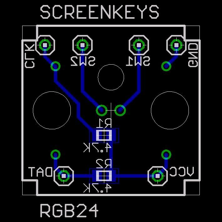
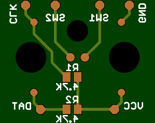
MarkS wrote:So, if I make a mistake during the CAM processing and upload that to the BatchPCB site and then catch the mistake (passed the DRC test), what do I do? I re-uploaded the corrected version, but never got the DRC check email for it.
Greetings Mark,

Having been in that position myself I strongly suggest an email to
SFE/Batchpcb to cancel the project that you have corrected.

Next, start a new Batchpcb project with the corrected data.

Batchpcb processes a lot more bot submissions than actual
paying customers that order PCBs (because many of us do
make mistakes or experiment with PCB design and wish to
see if it will pass the bot).

It is easier for them to cancel a project (and issue a credit)
than have to adjust to a revision later.

I'd also suggest that you mark your design in a way that
can be readily identified as revised. I use X1, X2, etc. until
the design hits production (then A, B, etc.).

Comments Welcome!
By MarkS
#35806
The problem is that I cannot seem to correct the file. The Eagle file I uploaded is for a ScreenKeys breakout board. You can see the design in my thread in the new products forum. The traces, two pull-up resistors and silk screen are on the back of the board and I cannot get it to look right when I run the CAM processor.
User avatar
By bigglez
#35808
MarkS wrote: The traces, two pull-up resistors and silk screen are on the back of the board and I cannot get it to look right when I run the CAM processor.
Mark,

I don't understand your issue, can you post your EAGLE files here?

Have you used BatchPCB before? Are you using the CAM processor
from SFE/BatchPCB to generate the production (Gerber) files?

Comments Welcome!

Peter
By MarkS
#35809
bigglez wrote:
MarkS wrote: The traces, two pull-up resistors and silk screen are on the back of the board and I cannot get it to look right when I run the CAM processor.
Mark,

I don't understand your issue, can you post your EAGLE files here?

Have you used BatchPCB before? Are you using the CAM processor
from SFE/BatchPCB to generate the production (Gerber) files?

Comments Welcome!

Peter
I followed the Eagle instructions on the BatchPCB site. I cannot post the files here since there is no way to attach them to a post. :(

Here is what the board looks like in Eagle:

Image

You're looking at the top of the board, but all of the traces, both resistors, and silk screens are on the bottom of the board. However, this is what BatchPCB is giving me:

Image

Not only is the board bigger that the Eagle dimensions layer, but the traces and silk screen is on the wrong side.

The obvious solution is to mirror the ScreenKey and draw the traces on the top of the board, but I'd like to know why this is happening and how to correct it.
User avatar
By bigglez
#35811
MarkS wrote:I followed the Eagle instructions on the BatchPCB site.
You're looking at the top of the board, but all of the traces, both resistors, and silk screens are on the bottom of the board. However, this is what BatchPCB is giving me:

Not only is the board bigger that the Eagle dimensions layer, but the traces and silk screen is on the wrong side.
Mark,

The image does not look 'wrong' to me. This is the composite image
that BatchPCB uses to identify your board in your BatchPCB account.

There should be two more files sent to you via email. The files are titled:
xxx-GTL.jpg and xxx-GBL.jpg These are jpg images of the the top and bottom Gerber files.

The composite image is missing the board outline, which is most likely an
error in your EAGLE design.
MarkS wrote: The obvious solution is to mirror the ScreenKey and draw the traces on the top of the board, but I'd like to know why this is happening and how to correct it.
I wouldn't do that, it's much better to get it right the first time. Even
a simple project like this one will take just as long to build and
much longer to fix if it's wrong. My time is better spent fixing the
flow than hoping the outcome is useable.

Go back to your EAGLE board design and determine which layer
has the outline (should be layer 20). Rebuild the project and sent
it again.

Comments Welcome!