SparkFun Forums 

Where electronics enthusiasts find answers.

Questions relating to designing PCBs
By CommanderBob
#30797
It says on the FAQ that there has to be 8mil clearence. I want to use a TQFP 80 pin but it says the clearence is 7mil so when I set it to 8mil I get an error so I click delete but the error still occures. Please help me. I am using Eagle and this is my first major board.

Thanks,
Justin
By propellanttech
#30802
Justin,

I can't speak for Dave Carne (the person who will answer your question) , but I believe that the clearance is not associated with the SMT pads.

I think you will have to have the error message......because eagle looks at the pads for clearance.

This is one of those instances that you will have an error in Eagle, but not a problem with having the board made.

James L
User avatar
By bigglez
#30826
CommanderBob wrote:It says on the FAQ that there has to be 8mil clearence. I want to use a TQFP 80 pin but it says the clearence is 7mil so when I set it to 8mil I get an error so I click delete but the error still occures. Please help me. I am using Eagle and this is my first major board.
Justin,

Clearance refers to the space between adjacent metal. (Pad to pad; pad to trace; trace to trace). BatchPCB has set a limit of 8mil, which guarentees functioning boards from their service.

The vendor in China can do much better, so you can take a chance that your board with 7mil clearance will run through correctly and work. There's a risk it won't. You have to take the risk - if the board is dead you can't blame SFE or BatchPCB.

First, set your EAGLE DRC limits to 7.00 mil and run it. Once you have no errors submit the board to BatchPCB, where it will likely fail the bot. If it passes, make a note with your order that you are taking a risk and the board should be fabbed. If it fails the bot, send email to BatchPCB pleading your case to run the board "as-is".

Plan B: send your Gerbers to another fab.

Comments Welcome!
User avatar
By phalanx
#30829
Another thing I would suggest is making your own TQFP package. Even the smaller 12mm x 12mm TQFP from Microchip (0.5mm pitch) will work with room to spare. The nominal pitch is 20mils and the maximum pin width is 11mils. That means even if you use 11mil traces going to the pins you will still have 9mils of clearance between traces and pads.

I've run a few 0.5mm boards through Sparkfun and never had an issue but I've always made my packages from scratch because I don't trust the ones included with Eagle.

-Bill
By CommanderBob
#30833
I just noticed that if I zoom in real close when I click check then little red lines appear between the pads and the error circles those lines. If I click delete all they disappear, but if I click check again they come back. I think it is just a glitch and if I click delete all then it should work.

Thanks,
Justin
By Philba
#30855
Uh, do you mean delete in the box that comes up when you get check errors? If so, you can delete any error or warning but all that does is remove the marks on the display. The errors are still there. I'm pretty sure it's not a glitch (i.e. not really an error). When you set clearance to be 8 mil, it flags anything that is less than 8 mil.
By CommanderBob
#30859
No, I mean if you zoom in on the pads of the chip and you check for errors then it circles little lines that appear. I will take a screen shot of I can and post it.
By CommanderBob
#30861
I can't figure out how to post pictures so...[/img]
By CommanderBob
#30862
Image[/img]

Here it is see the line that is circled?
By b_w_
#30864
Thats Eagles way of highlighting the problem areas with the DRC check, in your case the pad clearance problem. AFAIK you would need to set the tolerance to 7mil (again in your example) and rerun the drc to make it go away. I could be wrong...


-Brian
By Philba
#30896
again, clicking delete doesn't do anything than remove the indication on the display. any errors will still be there, just not showing.
By CommanderBob
#30901
Is it normal for the little red line to appear between the pads? I understand that clicking delete does nothing. Can you see the red lines?
User avatar
By bigglez
#30904
CommanderBob wrote:Is it normal for the little red line to appear between the pads? I understand that clicking delete does nothing. Can you see the red lines?
Greetings CommanderBob,

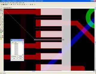
Only if the DRC finds a rule violation. Pads and traces can be placed anywhere, the DRC tool checks the placement against rules (clearance, drill size, trace angle, trace width, pad size and that all features are on grid, etc).

Changing to rules (or not running DRC) will avoid these errors. That also reduces the chance of the PCB being built correctly.

EAGLE flags the errors with an outline and cross-hatching, in the same colour as the layer. In this case the error is so small the outline has collapsed to a single line.

Clicking delete (in the DRC popup window) removes the current flag. Useful if the error has been fixed, or deliberately ignored. All DRC flags can be deleted at once.

Ideally, running DRC should generate "DRC:No errors". This is probably the most important step in the PCB design cycle!

Comments Welcome!
By CommanderBob
#30910
Thank you I think I will try my luck and just use that piece. Thanks for all the help.
By TruAnRksT
#31378
I agree with the guy who said make your own footprints. You can make the pads only slightly narrower and it will increase the clearance enough to meet the fab requirements while remaining a perfectly serviceable board. Could also help reduce solder bridges.

I believe Advanced only requires a 5 mil clearance so the suggestion to take your files to another shop is also valid.

It's kinda funny, when using the default .ttf in eagle I always get a report back with 1000's of line width violations on the silkscreen layer from the bot at Advanced. But if ignored (as they always are) all the text turns out perfectly legible anyway.