Page 1 of 1
Part clearance
Posted: Tue May 08, 2007 2:04 am
by futrtrubl
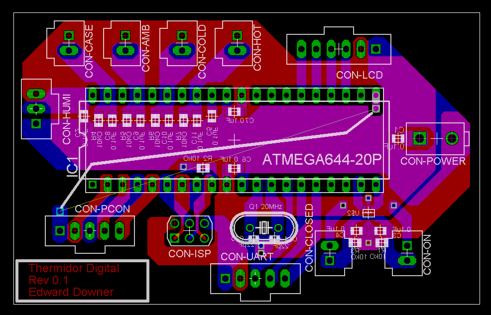
I'm working on the following board and I'm wondering how close I can bring the connectors to the uC.
The atmega644 is in a socket, the box around it shows the socket's outer dimensions. The connectors are all shrouded and the white lines are their outer dimmensions. For a sense of scale the connectors (except power) and the chip are all 100mil pitch.
Edward
Posted: Tue May 08, 2007 7:32 am
by phalanx
Technically you can move your connectors right to the edge of the through-holes on the pads for your microcontroller. Realistically you need to leave yourself enough room to get a soldering iron in there in case you need to rework items. It is an imperfect science that will take some experience to get right. To this day, I still tend to overestimate how much room I need between devices. Once i start putting the board together I realize that I could have moved parts much closer together and saved money on the PCB.
What you can do is print out your PCB on paper (1:1 scale) and place your parts on the printout to see how they all line up. You will then have a better idea of what you can and cannot do to tighten things up.
Also, are you intending to use a wire to make a connection from CON-PCON to pin 21 of your controller? There is no reason why you couldn't make that a copper trace. If you are worried about splitting your power or GND pours, run part of the trace on the top layer and part on the bottom so the split isn't as significant.
-Bill
Posted: Tue May 08, 2007 10:28 am
by futrtrubl
What you can do is print out your PCB on paper (1:1 scale) and place your parts on the printout to see how they all line up. You will then have a better idea of what you can and cannot do to tighten things up.
Great idea, I should do that anyway to make sure my pads line up properly for my parts.
Also, are you intending to use a wire to make a connection from CON-PCON to pin 21 of your controller? There is no reason why you couldn't make that a copper trace. If you are worried about splitting your power or GND pours, run part of the trace on the top layer and part on the bottom so the split isn't as significant.
That's what I'm intending. Even if I run part on the top and part on the bottom I'll still halve the width of 1 or both pours.
Edward
Posted: Tue May 08, 2007 11:48 am
by phalanx
futrtrubl wrote:That's what I'm intending. Even if I run part on the top and part on the bottom I'll still halve the width of 1 or both pours.
Edward
Why not run a trace around the outside of the board? When you get to the CON-LCD connector, run the trace on the backside between pins 2 and 3 then connect it right to pin 21 on your controller. An 8mil trace will fit just fine and you would not have to split your power and GND pours.
-Bill
Posted: Tue May 08, 2007 9:42 pm
by SOI_Sentinel
Split? He's got a figure 8 around the entire upper set of pins.
You could wipe out the entire Vdd power plane underneath the chip and still have plenty of copper to go around, and still have a continuous ground and power pour.