SparkFun Forums 

Where electronics enthusiasts find answers.

Questions relating to designing PCBs
By buffavaholic
#157465
Hi,

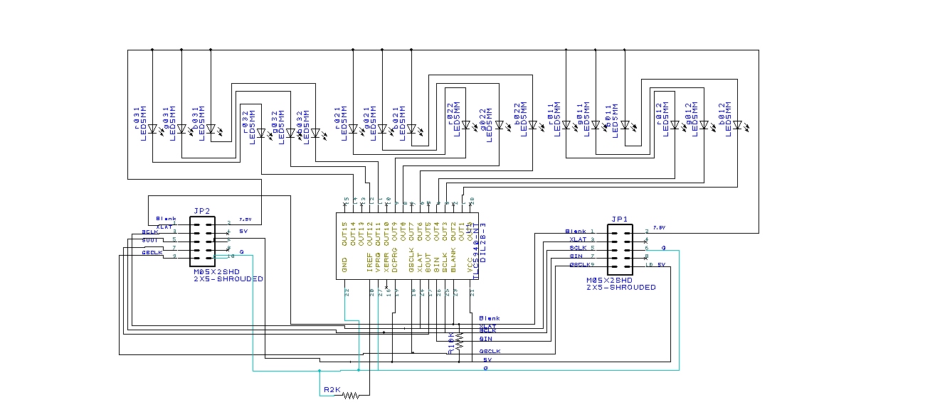
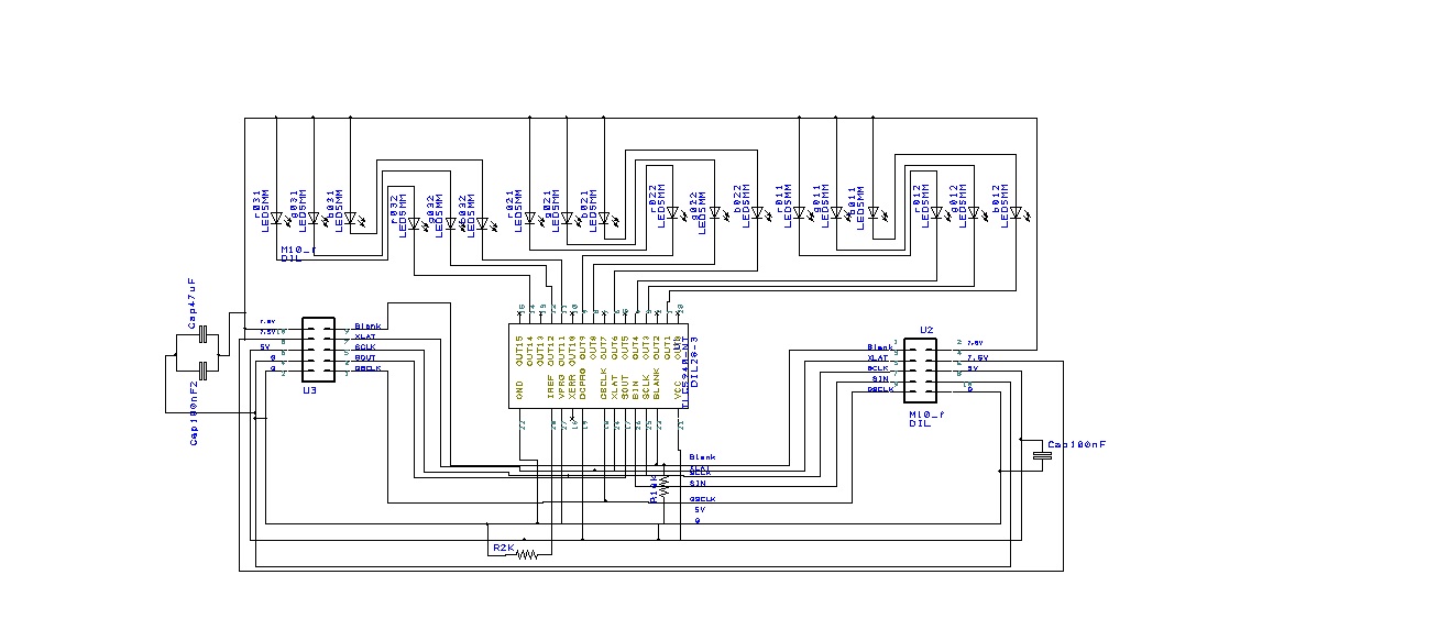
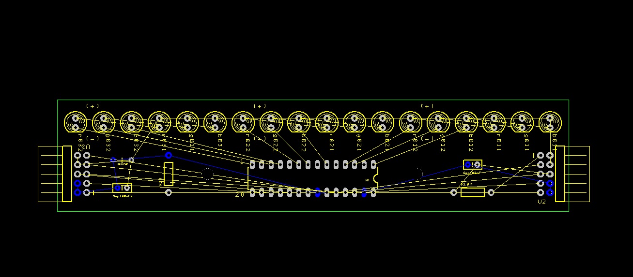
I am fairly new to electronics and very new to PCB design. I am trying to create a row of LEDs that are RGB controlled in small segments using a TLC5940 to either make downlighting or for lighting artwork for different effects. I will be daisy chaining up to 10 together, but I want to design my PCB to have both the LEDs and the TLC5940 on one PCB and then be able to connect to additional copies of the PCB. So all these PCBs need to lay flat in the same plane. How can I best connect PCBs to each other for this? Right now I have thrown in a shrouded 10 pin header which i could connect via ribbon wire (https://www.sparkfun.com/products/8506). but this seems like it is unnecessary and large. I need 8 pins at least. What other options are there?

The image of my schematic can be seen in the link below.

Thanks!

http://beerandelectrons.files.wordpress ... schem2.jpg
By n1ist
#157491
They make the female version of the right-angle 10-pin header as well, so by putting a male header on one end of the board and a female header on the other end, you can connect the boards in line. Alternatevely, you can just put pads on the edge of the board and solder wires between them. If you are using 10-pin headers, I'd add another 7.5v pin and ground pin to reduce voltage drop.

Also, I'd add a 100n bypass cap on the 5v rail and 100n in parallel with a 47u or 100u on the 7.5v rail to reduce noise issues.

/mike
By buffavaholic
#157573
Thank you for the advice Mike! Using right angle headers was my first idea, but I am having a hard time finding one that is included in a library compatible with Designspark. I guess I will have to not be lazy and add the components in myself. As for adding the capacitors, were the capacitance you listed based on equations or heuristics? If you have a textbook that you find particularly helpful for things let me know and I'll check it out.

Thanks again for your help.
By Garth
#157575
but I am having a hard time finding one that is included in a library compatible with Designspark. I guess I will have to not be lazy and add the components in myself.
I think it is pretty much assumed that for any CAD package, you will have to add library parts yourself. There are simply way too many possibilities for them all to be included in one CAD, and even if they could, new ones are coming out all the time. I've had to make hundreds over the years.
By n1ist
#157651
Those cap values were just guesses. 100n is common for bypass caps (sometimes in parallel with 10n if you have lots of high frequency noise around, or 1u if the chip is rapidly switching large currents). As for the bulk cap, yes, you can calculate that based on number of LEDs, current draw, and switching frequency.
/mike
By buffavaholic
#157812
Thank you for the comments! I have found a suitable pair of headers that I think will do the trick (Male header female socket)

I have also added the 100nF and parallel 100 nF and 47 uF bypass capacitors to the 5v and 7.5v lines respectively. Also I used the two extra pins to add an additional 7.5v and G lines. I am assuming that I connect the two 7.5v lines and two ground lines together right?

The updated image schematic can be found here:
Schematic Image

And my PCB layout image can be found here
PCB Layout Image

Thanks!
E
where both links are from my blog http://beerandelectrons.wordpress.com/
By buffavaholic
#158016
After looking at the design, I think the way I put in the extra 7.5v and ground rails doesn't make sense because now there is just a copper connection between the pins. I am assuming I need to put some resistor between the two rails, but will any resistor do?
By Garth
#158030
I'm not sure where you think you need resistors. The details of the diagram are so small they kind of get lost in the pixels, but it looks ok to me. For something like this, it is normally best to distribute the pins that are ground or a power supply or reference voltage that is bypassed to ground so the conductor carrying the return current for any given signal pin is as close as possible, and you already have that.

The next thing to do is use a ground plane. For digital signals with a high slew rate, this does not mean a pour. Pours are rather worthless in digital work. Keep in mind that with a real ground plane, the return current for any given trace does not follow the widest, shortest path, but instead the mutual inductance makes the return current in the ground plane try to go directly underneath the trace, taking on the shape of the trace. This makes for the best AC performance. If the trace crosses an interruption in the ground plane (like you would get at the edge of a pour), now the return current must go around, and you basically have a portion of a coil. Antennas are made this way in cell phones sometimes. That's why copper pours do not qualify as a ground plane in digital work. It won't matter so much for a really small board, but it sounds like you're going to have quite a string of these things. If you have only two layers to work with and you need a jumper, you might choose a manually inserted wire, or, if you really must cut into the ground plane to put a jumper in, make it as short as possible.
Last edited by Garth on Fri Apr 12, 2013 8:52 pm, edited 2 times in total.
By buffavaholic
#158092
For now I am trying to make this a 2 layer board to keep the cost down, so I don't think I will be able to do a ground plane. I am going to have at most 10 boards connected in series.
n1ist wrote: If you are using 10-pin headers, I'd add another 7.5v pin and ground pin to reduce voltage drop.
So when I did this I just directly connected the ground pin coming in directly to the ground pin going out, and then connected that bypassed ground rail to the other ground rail. But when this is converted into the PCB design, it really just connects the two pins together at the header, then I don't see how that would reduce the voltage drop across a board. Unless I have it wrong and we are trying to reduce a voltage drop across a header. I thought maybe if I put a small resistor between the two ground rails this would actually keep them as separate tracks. Or is that I just need to force a direct track in the PCB? (I have been letting designspark optimize all the nets)
A zoomed in detail of the connections to the headers and between rails can be seen below.
LEDschemdetail (1280x561).jpg
Thank you for the help,

E
You do not have the required permissions to view the files attached to this post.
By Garth
#158110
There is a time to isolate grounds, and I deal with it when our customers install our communications and entertainment equipment in aircraft and they think ground is ground is ground and end up with buzzes and whines in the audio, and I have to explain again why the grounds of audio connectors cannot have a direct connection to the airframe but instead get their only ground connection through the ground conductor in the cable leading to them.

This is a different situation. Just tie the two pins together and have them both go to a ground plane, and make the signal lines have a continuous ground plane under them. If the IC had separate grounds for input signal versus the LEDs' cathode current, then it would make sense to seaparate the grounds; but it doesn't have separate grounds pins. If it did, the idea would be to keep big changes in total LED current from altering the voltage against which the input signals are referenced, as there would be some voltage drop across the LED ground connection. Apparently the designers decided that the shift in how much voltage is dropped across the ground connections would not be enough to matter on digital logic inputs, and they did not give the IC separate grounds.
By n1ist
#158145
The idea is to have the two pins in parallel. It reduces the contact resistance and increases the current-handling capacity. One trace or pour hits both pins.
/mike
By buffavaholic
#158147
Ok, thanks! I would need quite a few jumpers for this design to make a two layer board with one layer being ground. I think I will go forward with the design I have and hope for the best, I am guessing when I just have one board connected I won't see any problems but we'll see when I have 10 in series.

Thanks for all the suggestions.
E
By n1ist
#158213
I would run a fat trace (150 mils or wider) for 7.5V, starting at the left connector, going up over the top of the LEDs, to the right side. If you can't do a pour for ground, at least run a similar wide trace along the bottom of the board. The trace can be stubbed down to 50 or 100 mils for the very short distance between the main trace and connector pins. Remember, worst case (all LEDs on), you will have about 3.2A (20mA per LED * 16 per board * 10 boards) flowing through the first board...

+5 doesn't need to be as wide but since you have the space (it can run bottom side between the LEDs and IC if the other traces are topside), I'd do 50 mils to reduce the inductance.

The decoupling caps will need to be moved to right next to the Vcc pin of the TLC5940.

For this board, I would route the 5 control traces plus +5V between the LEDs and IC horizontally on the bottom, dropping vertical top-side traces from them down between the top row of IC pins to the bottom row where they need to go. That would leave the bottom of the board available for a nice ground pour.

/mike