- Sat Jan 28, 2017 10:32 pm
#193146
Dear Sparkfun,
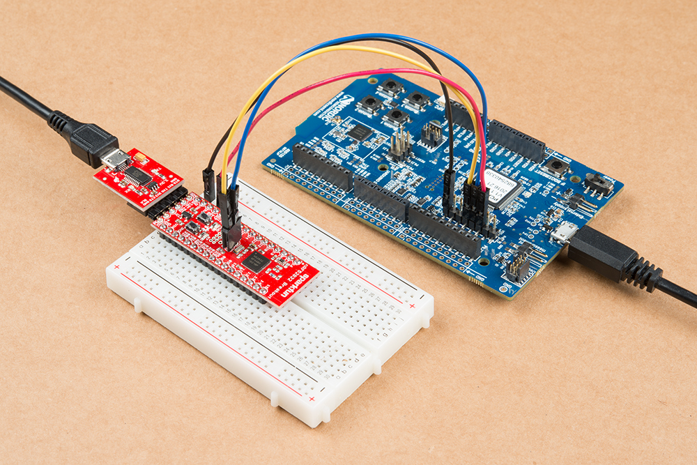
I attempted to hook up my nRF52832 board to a Segger J-Link (on an nRF52 Explorer) using the schematic and mirroring the connection shown in this product walkthrough photo:
https://cdn.sparkfun.com/assets/learn_t ... -board.jpg
The test point labeling on the board is ambiguous; it isn't apparent which point is TP1 and which isn't. The photo shows the nRF52 Explorer SWDIO and SWCLK connected to the transverse 0.1" pins closest to the microcontroller. However, with the benefit of hindsight and hours of suffering, I can confidently say that those points are not SWDIO and SWCLK. The two slightly smaller holes between those and the CMSIS connector are TP1 and TP2.
For the benefit of other users, I beseech you to replace that deceptive photo in the product walkthrough with another that shows the correct J-Link wiring. It would also be great if you posted a geometric pinout in addition to the abstract schematic.
Thanks!