- Wed Dec 28, 2011 3:00 pm
#137523
Hi, this is my first post on this forum and I'd like you to be forgiving to my english because it's far from perfect. Nevertheless, I hope I will be understandable for you.
My problem concerns the tim1's configuration from DSO nano project. I'd like to use this configuration in my hobby project. I assumed it is well-thought-out and it would be appropriate in my simple osciloscope.
Here is the original configuration:
I found somewhere that period of such configuration is (PSC+1)*(ACC+1)/system clock . Unfortunately I dont understand enough conception of this configuration and I'm wondering what is the meaning of CCR1 register (I know only that it defines a width of PWM's pulse) but what is the infulence of this parameter on frequency of events?
I'm also trying to guess what the autor had in mind creating this code. ADC1 (which is ivoked by TIM1's events) invokes DMA which stores sample value in memory after convertion. If so, why in TIM1's configuration are set bits TIM_DIER_CC1DE, TIM_DIER_UDE, TIM_DIER_TDE? I assume there is deeper meaning but at present I see this configuration works like this:
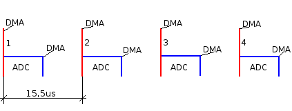
vertical lines are events. The time which is the period was calculated form this equation (PSC+1)*(ACC+1)/system clock (30+1)*(35+1)/72MHz
I'm sure I'm wrong in my thinking. From this picture follows that DMA at beggining of second event should store the same value as DMA invoked by first ADC convertion.
As I mentioned earlier I tested this configuration and I noticed that gathered values side by side are not equal.(so Im wrong) On the one hand it has sense because there is no DMA's chanel configured for tim1. If so, why in DSO nano in TIM1 configuration are set bits to DMA transactions?
My problem concerns the tim1's configuration from DSO nano project. I'd like to use this configuration in my hobby project. I assumed it is well-thought-out and it would be appropriate in my simple osciloscope.
Here is the original configuration:
Code: Select all
Rewrited form above code (maybe for someone more readable format):
TIM1->PSC = 60; //ex. value
TIM1->ARR = 35; //ex. value
TIM1->CCR1 = (35+1)/2;

TIM1->CR1 = 0x0094;/*0000 0000 1001 0100
                      |||| |||| |||| |||+---CEN=0
                      |||| |||| |||| ||+----UDIS=0
                      |||| |||| |||| |+-----URS=1
                      |||| |||| |||| +------OPM=0
                      |||| |||| |||+--------DIR=1
                      |||| |||| |++---------CMS=00
                      |||| |||| +-----------ARPE=1
                      |||| ||++-------------CKD=00
                      ++++-++---------------Reserved*/
TIM1->RCR = 0x0000;/*0000 0000 0000 0001   Repetition counter register
                      |||| |||| ++++ ++++---Repetition Counter Value=1
                      ++++-++++-------------Reserved*/
TIM1->CCER =0x0001;/*0000 0000 0000 0001
                      |||| |||| |||| |||+---CC1E=1
                      |||| |||| |||| ||+----CC1P=0
                      |||| |||| |||| |+-----CC1NE=0
                      |||| |||| |||| +------CC1NP=0
                      ++++-++++-++++--------Reset value*/
TIM1->CCMR1=0x0078;/*0000 0000 0111 1100
                      |||| |||| |||| ||++---CC1S=00
                      |||| |||| |||| |+-----OC1FE=1
                      |||| |||| |||| +------OC1PE=1
                      |||| |||| |+++--------0C1M=111
                      |||| |||| +-----------OC1CE=0
                      ++++-++++-------------Reset value*/
TIM1->BDTR =0x8000;/*1000 0000 0000 0000
                      |+++-++++-++++-++++---Reset value
                      +---------------------MOE=0*/

TIM1->DIER =0x4200;0100 0011 0000 0000  DMA/Interrupt enable register
                       |     ||        +----CC1IE=0
                       |     |+-------------UDE=1
                       |     +--------------CC1DE=1
                       +--------------------TDE=1

TIM1->CR1 |=0x0001;//CEN=1, TIMER1 EnableCode: Select all
In general, the aim of this configuration is to set TIM1 to be trigger for ADC (events trigger ADC's convertions). I even take some experimets with this piece of code and it works. My problem is that I'm not able to precisely define the period of ocurring events and invoked ADC's convertions. TIM1->PSC = 30;
TIM1->ARR = 35;
TIM1->CCR1 = (35+1)/2;
TIM1->CR1 = TIM_CR1_DIR | TIM_CR1_URS | TIM_CR1_ARPE;
TIM1->RCR = 0x0000;
TIM1->CCER = TIM_CCER_CC1E;
TIM1->CCMR1 = TIM_CCMR1_OC1FE | TIM_CCMR1_OC1PE | TIM_CCMR1_OC1M;
TIM1->BDTR = TIM_BDTR_MOE;
TIM1->DIER = TIM_DIER_CC1DE |TIM_DIER_UDE | TIM_DIER_TDE;
TIM1->CR1 = TIM_CR1_CEN;I found somewhere that period of such configuration is (PSC+1)*(ACC+1)/system clock . Unfortunately I dont understand enough conception of this configuration and I'm wondering what is the meaning of CCR1 register (I know only that it defines a width of PWM's pulse) but what is the infulence of this parameter on frequency of events?
I'm also trying to guess what the autor had in mind creating this code. ADC1 (which is ivoked by TIM1's events) invokes DMA which stores sample value in memory after convertion. If so, why in TIM1's configuration are set bits TIM_DIER_CC1DE, TIM_DIER_UDE, TIM_DIER_TDE? I assume there is deeper meaning but at present I see this configuration works like this:
vertical lines are events. The time which is the period was calculated form this equation (PSC+1)*(ACC+1)/system clock (30+1)*(35+1)/72MHz
I'm sure I'm wrong in my thinking. From this picture follows that DMA at beggining of second event should store the same value as DMA invoked by first ADC convertion.
As I mentioned earlier I tested this configuration and I noticed that gathered values side by side are not equal.(so Im wrong) On the one hand it has sense because there is no DMA's chanel configured for tim1. If so, why in DSO nano in TIM1 configuration are set bits to DMA transactions?